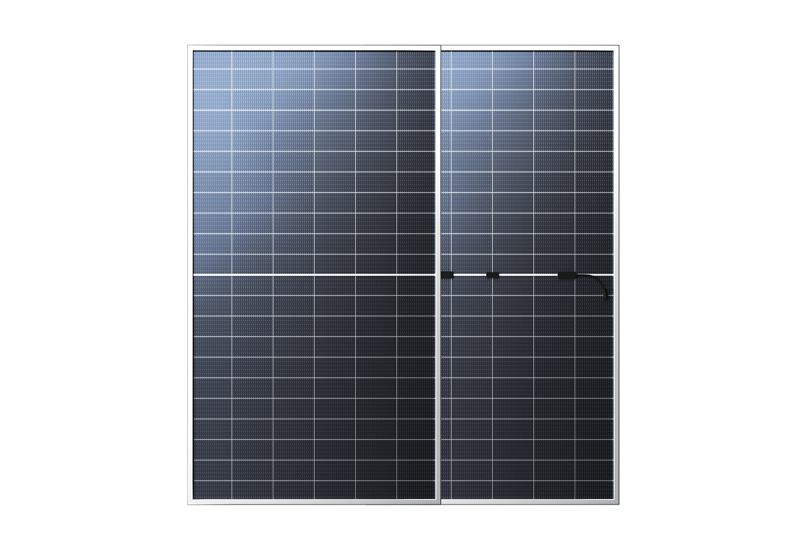
HJT Product
G12-18BB HJT Solar Cell
Wafer type: N-type monocrystalline silicon wafer
Size: 210 * 105 ± 0.25mm
Thickness: 110±15μm
Max. Power of Half Piece: 5.61W
Max. Efficiency: 25.50%
G12-20BB HJT Solar Cell
Wafer type: N-type monocrystalline silicon wafer
Size: 210 * 105 ± 0.25mm
Thickness: 120 ± 15μm
Max. Power of Half Piece: 5.61W
Max. Efficiency: 25.50%
Advantages of HJT Solar Cell

1
Higher Power Conversion Efficiency
HJT solar cell uses amorphous silicon thin films as passivation materials to reduce the loss of minority carriers lifetime in contact area, which could increase the open circuit voltage of HJT cells to 750mV and guarantee the power conversion efficiency up to 25% at the beginning. With bifacial microcrystals can further improve the doping efficiency and transmittance of the thin films, improve current density, and thereby improve cells conversion efficiency up to 25.2%.

2
Thinner Wafer Adapted
The manufacturing process of HJT solar cell is simplified comparing with conventional solar cells, with low temperature process, its natural bifacial symmetrical structure have reduced the mechanical stress in cell production, which enable to realize a thinner wafer ( ≤120um). Combining with SMBB technology and 0 Busbar technology, the conversion efficiency can be further improved and costs reduced.

3
Lower Power Degradation Rate
HJT solar cells is made of N type silicon wafer, which does not have B-O bound, resulting in no LID effect, guarantee long term durability. As anti-reflection and protective layers, TCO film is conductive, so the charge won’t polarize on the surface, avoiding PID from the structure.

4
Lower Temperature Coefficient
Temperature coefficient is one of the important parameters of PV modules, which will affect the power generation of the modules. HJT solar cell temperature coefficient is
-0.26%, only half of the temperature coefficient comparing with crystalline silicon cells
-0.45%. So HJT has a greater advantage in high temperature, high irradiation area. In the case of summer hot climate, HJT generates 6% more power than conventional monocrystalline cells, and 3% more power than TOPCON cells.

5
Higher Bifacial Rate
HJT solar cell has natural bifacial symmetric structure, and the bifacial rate is more than 95% on average, which could be adapted to different application scenarios, and gain more power output.

6
Ultra-low Carbon Footprint
HJT solar cell have a Simplified process flow, low manufacturing temperature, high power conversion efficiency, and adopt a thinner wafer, which enable to reduce energy consumption and achieve a lower carbon footprint.

